Invited Speakers
Dr Rachael Myers-Ward
US Naval Research Laboratory, USA
Remote Epitaxy The Future for Stackable SiC Electronics
Rachael Myers-Ward is an electrical engineer in the Power Electronics Branch/ Power Electronic Materials Section at the U.S. Naval Research Laboratory. She received a Ph.D. in electrical engineering in 2006 and B.S. and M.S. degrees in chemical engineering in 2001 and 2003, respectively, from the University of South Florida. Her research interests include epitaxial growth of SiC via chemical vapor deposition for high power/high voltage device applications and quantum sciences, investigations to reduce extended and point defects in SiC epitaxial layers, and synthesis of epitaxial graphene for sensor applications.
Session: MO.02 4H-SiC epitaxy new trends
Dr Mermet- Guyennet
Supergrid Institute SAS, France
Potential of SiC devices in MVDC and HVDC converters for Grid: application requirements and reliability validation standards
Michel MERMET GUYENNET was born in 1957. He holds PhD (1984) in Applied Physics from Université de Marseille-Luminy  and graduated from Ecole Centrale de Paris (1981). He successively worked for Thomson Militaire et Spatial, SGS-Thomson, Advanced Computer Research Institute and Compagnie des Signaux where he was in charge R&D programmes in the field of electronic components and system hardware. He joined ALSTOM Transport in 1996 in charge of technology development for IGBT power converters for traction. From 2001 to 2010, he was Technical Director of Pow ofer Electronics Associated Research Laboratory (PEARL). From 2011 to 2013, he was in charge of development of full SiC converter with high speed motor. He is now with Supergrid-Institute in Villeurbanne as Director of Program Power Electronics & Converters. He supervises development of 10kV SiC BJT and PiN diodes and stability-robustness assessment of SiC MOSFET.
Session: MO.03 Applications
Mr Shunsuke Asaba
Toshiba Corporation, Japan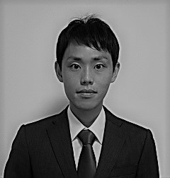
Interface Reaction in the High-temperature N2 Annealing Process for Gate Insulator on SiC with High-Mobility and High-Reliability
Shunsuke Asaba received a masters degree from Nagoya University, Japan in 2014. He joined Toshiba Corporation as a researcher and is involved in R&D of wide-bandgap semiconductor devices. In his current work on SiC-MOSFET, he studies MOS process technology.
Session: TU.01a MOS Interface Processing
Dr Nicolò Piluso
STMicroelectronics, Italy
High quality 4H-SiC epitaxial layer by tuning CVD process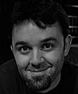
Nicolò Piluso was born in Catania, Italy, in 1979. He received a B.S. degree in physics from the University of Catania, Catania, in July 2004. In March 2008 he received a Ph.D. in physics from the University of Catania, studying the magnetic activity in late-type stars. From July 2008 to December 2009, he attended the SiCilab training project, for the “Training of experts in the growth of high gap semiconductors” organized by the Institute of Microelectronics and Microsystems, National Research Council (CNR–IMM), Catania. From April 2010 to December 2011 he worked for CNR-IMM as “post-doctoral fellowship”. In 2012, he worked in the R&D department of Epitaxial Technology Center s.r.l. From 2013 to 2014 he worked for CNR-IMM as “post-doctoral fellowship”. Starting from 2014 he works for STMicroelectronics s.r.l. in R&D group.
His main research activity is dedicated to SiC epitaxial growth and optical characterization. His research also include study of ion implantation process, thermal process, defects characterization and electrical evaluation of power devices. He is member of IEC (International Electrotechnical Commission); he was nominated expert for SiC material in 2017. He published more than 80 articles in scientific journals and International conference proceedings.
Session: TU.01b 4H-SiC epitaxy
Dr Edward Van Brunt
Wolfspeed, A Cree Company, USA
Industrial and Body Diode Qualification of Gen-III Medium Voltage SiC MOSFETs: Challenges and Solutions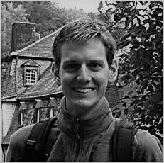
Edward Van Brunt joined Cree in 2013 as a Research Scientist. He received his BSEE degree from the University of Texas at Austin in 2007, and received his MS and Ph.D. in electrical engineering from North Carolina State University in 2009 and 2012, respectively. He has authored or co-authored more than 55 papers, and holds 8 US patents. Edward’s research interests include high voltage SiC device development and processing, as well as defect analysis in 4H-SiC wafers.
Session: TU.02a Power MOSFET
Professor Antonella Parisini
University of Parma, Italy
Carrier transport mechanisms in highly-doped p-type 4H-SiC(Al)
Antonella Parisini is Associated Professor of the University of Parma since December 2004. Her main expertises concern the study of basic electronic properties of compound semiconductors, by optical, photoelectrical, transport investigation, in particular: (i) III-V epitaxial single and multi- layers, consisting in both 3D and quantum confined 2D structures, aimed to applications in electronics, optoelectronics, photovoltaics; (ii) bulk structures of wide-bandgap semiconductors, in particular ion-implanted 4H-SiC, finalized to devices for power electronics, and, more recently, group III-sesquioxides, in particular β- and ε- Ga2O3 polytypes.
The physical properties of wide-bandgap semiconductors and their potential applications for power electronics constitute her current main research interest, particularly focused on electrical properties of the materials. She is co-author of more than 100 publications, including articles in international journals and conference proceedings, participated to several research projects and was member of the Organizer Committee of international congresses, in particular, regarding wide-bandgap semiconductors, of the International Workshop on Gallium Oxide and Related Materials IWGO2017 (12-15 September 2017, Parma, Italy).
Session: TU.02b Fundamental Properties
Professor Anders Hallén
Royal Institute of Technology, Sweden
Recent advances in the doping of 4H-SiC by channelled ion implantation
Professor Anders Hallén received his M.Sc. degree in electronic engineering in 1985 and PhD in ion physics in 1990 from Uppsala University, Sweden. He started at The Royal Institute of Technology, KTH, in 1996. Hallén's major research area involves material modification using ion beams, targeted on the electrical properties of semiconductor materials. He has also been associated with ABB, developing methods for charge carrier lifetime control for Si power devices, and later involved in SiC power device development. Since 2006 he is a professor at KTH, focusing on the development of SiC power devices. He was also highly involved in the formation of the Ion Technology Centre (ICT) in 2001, a Swedish national platform for the application of ion beams. His publication list includes over 200 articles in international journals and he has supervised 13 PhD students.
Session: TU.03a Ion Implantation
Dr Patrick Fiorenza
NR-IMM Catania, Italy
SiO2/SiC MOSFETs interface traps probed by nanoscale analyses and transient current and capacitance measurements
Patrick Fiorenza received an M.Sc. in Physics and a PhD in Material Science from the University of Catania in 2003 and 2007, respectively. In 2005, he was visiting scientist at IMEC (Belgium). Since 2011 he is permanent Staff Researcher at CNR-IMM. His research activity is mainly focused on carrier transport, trapping phenomena and reliability at MIS and MS interfaces in SiC and GaN. He has a recognized experience in characterization of advanced materials and devices by scanning probe microscopy. He is co-author of more than 120 papers and three book chapters. He was member of the local organizing committee of Hetero-SiC-WASMPE 2009, WOCSDICE2011 and ICSCRM 2015, and was involved in several European and national projects (NUOTO, NetFISiC , Last Power, Ambition Power, WinSiC4AP and CHALLENGE). He is principal investigator for the CNR-IMM unit of the project GRIFONE (2015-2018) within the FlagERA call.
Session: TU.03b MOS Interface Characterisation
Dr Naoyoshi Komatsu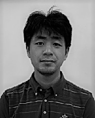
National Advanced Industrial Science and Technology (AIST)
Application of defect conversion layer by solution growth for reduction of TSDs in 4H-SiC bulk crystals by PVT growth
Dr Naoyoshi Komatsu is a research scientist at the National Institute of Avanced Industrial Science and Technology (AIST). He received his PhD degree in electrical engineering from Osaka University in 2011, based on his work on SiC devices and material characterization. He joined R&D Partnership for Future Power Electronics Technology (FUPET) in April of 2011, where he conducted solution growth of SiC bulk crystal based on optimization of solvents. Komatsu joined AIST from 2015, where his current research involves high quality SiC crystals by solution growth and related fundamental technologies.
Session: WE.01a Solution Growth
Dr Naoki Watanabe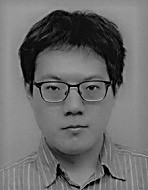
Hitachi, Ltd., Japan
Improvement of Switching Characteristics in 6.5-kV SiC IGBT with Novel Drift Layer Structure
Naoki Watanabe is a researcher in the Center for Technology Innovation Electronics at Hitachi, Ltd. He received his B.S. and M.S. in 2008 and 2010, respectively, and Ph.D. in Engineering in 2013 from Kyoto University, studying MEMS and sensors with wide bandgap semiconductors. His current research interests include SiC device physics and power electronics.
Session: WE.02a High Voltage Devices
Dr Kevin Matocha
Monolith Semiconductor, USA
Reliability and Ruggedness of planar Silicon Carbide MOSFETs
Kevin Matocha received a B.S. degree in electrical engineering from Louisiana Tech University, Ruston, LA, in 1995, and M.S. an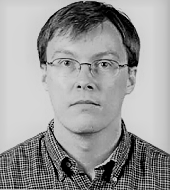 d Ph.D. degrees in electrical engineering from the Rensselaer Polytechnic Institute (RPI), Troy, NY, in 1998 and 2003, respectively. His doctoral work examined the capabilities of GaN MOSFETs for high-voltage switching applications. From 2000 to 2011, he was with the General Electric Global Research Center, developing wide-bandgap devices, including harsh environment sensors and power devices using silicon carbide and gallium nitride. He was a member of the team who received the 2009 Robert N. Hall Award, and was awarded the 2010 Albert Hull Award for his early career research. In 2011, he joined SemiSouth as Vice President of Product Development, commercializing SiC power devices including high-voltage SiC Schottky diodes and SiC JFETs. In 2012, he co-founded Monolith Semiconductor Inc., Austin, TX, a supplier of SiC Schottky diodes and SiC MOSFETs for power electronics applications, where he serves as Chief Technology Officer. His technical interest focuses on the performance and reliability of SiC MOS devices. Dr. Matocha has published 80 journal and conference articles, has authored one book chapter, and has been awarded 33 patents. He is currently an editor of IEEE Electron Device Letters.
Session: WE.03a Device ruggedness
Professor Ohtani Noboru
Kwansei Gakuin University, Japan
Key issues in physical vapor transport growth of SiC bulk crystals for power device applications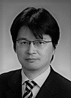
Noboru Ohtani is Professor of School of Science and Technology and Director of R&D Center for SiC Materials and Processes at Kwansei Gakuin University, Hyogo, Japan. He earned his PhD degree in 1993 from Imperial College London, UK. Prior to joining Kwansei Gakuin University, he was with Advanced Technology Research Laboratories, Nippon Steel Corporation from 1984 to 2008 after graduating from Tokyo Institute of Technology, Japan, where he obtained MSc degree in Physics in 1984. At Nippon Steel Corporation, he was responsible for leading several research projects on semiconductor materials and devices, particularly focusing on silicon carbide (SiC) semiconductor materials. For more than 25 years, he has pioneered and made seminal contributions to the development and manufacturing of large high-quality SiC single crystals and substrates.
Session: WE.03b PVT Growth
Masashi Nakajima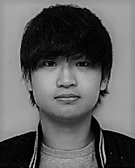
Dept. of Electronic Sci. Eng., Kyoto University, Japan
400°C operation of normally-off n- and p-JFETs with a side-gate structure fabricated by ion implantation into a high-purity semi-insulating SiC substrate
Masashi Nakajima received a B.E. degree from Kyoto University, Kyoto, Japan, in 2018. He is currently pursuring an M.E. degree with Kyoto University, Kyoto, Japan. His current research interests include fabrication and characterization of SiC JFETs.
Session: TH.01 Sic Integrated Circuit
Dr Lasse Vines
University of Oslo, Norway
Understanding and control of deep level defects in 4H-SiC: In Memoriam Bengt G. Svensson
Lasse Vines holds an Associate Professor position at the Department of Physics, University of Oslo. He received his Ph.D. from the University of Oslo in 2008, where he did his work in the group of Prof. Bengt G. Svensson. Vines research activity is focused on doping, defects, diffusion and ion beam modification in semiconductors; both in bulk, thin films and nanostructures, particularly related to materials such as silicon, silicon carbide and oxide semiconductors. His scientific expertise is mainly of experimental character and related deposition, and electrical and chemical characterization.
Vines has authored or co-authored >110 technical papers in refereed scientific journals and contributed to one book chapter.
Session: TH02 Contacts and Other Processing
Professor Jose Coutinho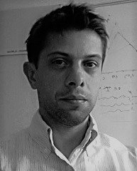
University of Aveiro, Portugal
Carbon vacancies and interstitials in 3C- and 4H-SiC: theoretical milestones and challenges
José Coutinho did his PhD in 2002 at the University of Exeter, United Kingdom, where he studied physics of defects in semiconductors with Bob Jones. He currently holds a position of Principal Researcher at the i3N Laboratory of the University of Aveiro in Portugal. His research interests span several topics, including physical problems in solar power conversion, in bio-functional and two-dimensional materials, in surface science or semiconductor detectors. He has been addressing problems in the above areas by means of atomistic modeling and electronic structure calculations using density functional and many-body perturbation methods.
Session: TH.03 Carrier Lifetime