
Ohmic Contact
The Ohmic contact is a low resistance junction (non-rectifying) provides current conduction from metal to semiconductor and vice versa. Theoretically speaking the current should increase/ decrease linearly with the applied voltage. With an immediate response for the any small voltage. There are two types of the Ohmic contacts:
-
The Ideal Nonrectifying Barriers
a) b)
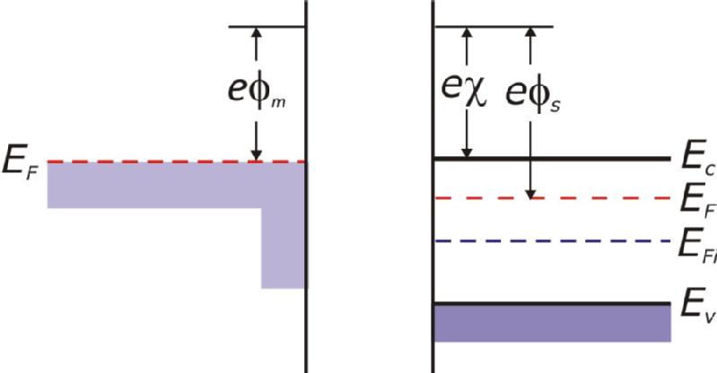
Figure 1: a) An ideal energy band diagram before contact
b) after contact for a metal -n- semiconductor junction for
In this type of contacts, after thermal equilibrium, which occurs when electrons flows from the metal to the semiconductor lower energy levels. These electrons flow back into the metal part if a positive bias in the metal part was applied, and they will feel no barrier. Applying a negative bias forces electrons to flow from metal to semiconductor seeing a very small barrier.
a) b)
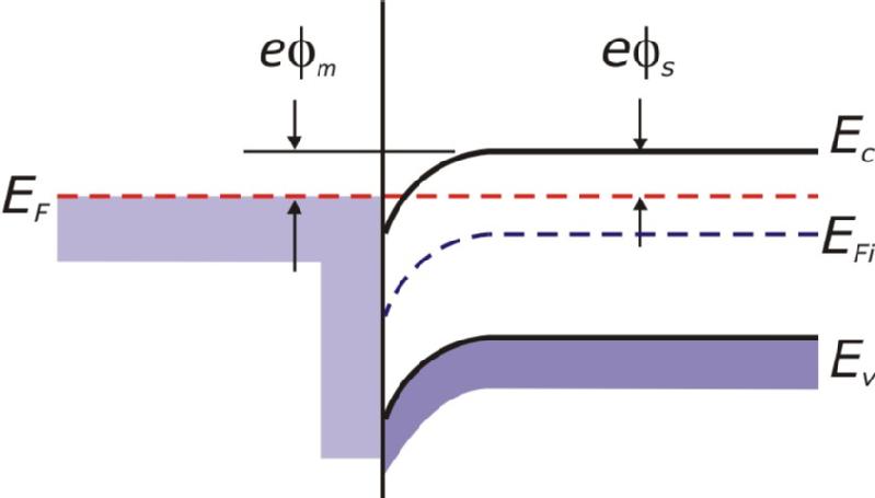
Figure 2: a) Ideal energy band diagram of a metal -n-type semiconductor ohmic contacts
a) positive bias to the metal, b) negative bias to the metal
As you can see from the figure 2a, applying a positive bias to the metal makes electrons to flow easily downhill, while negative bias makes the flow from the metal part to the semiconductor and this the picture of an Ohmic contact.
-
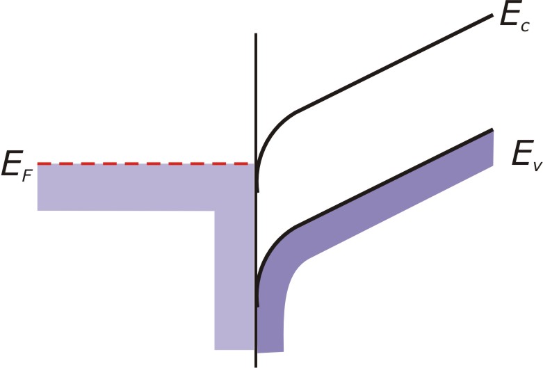
The Tunneling Barriers
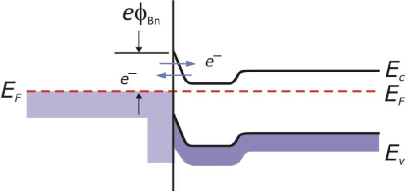
Figure3: An ideal energy band diagram of a heavily doped n-semiconductor -to - metal junction
Enhancing doping concentration in a semiconductor decreases the depletion region, which improves thetunneling probability throw the barrier.