
Schottky Contact
The rectifying contact that occur between a metal and a lightly doped semiconductor.
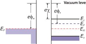
a) b)
Figure(1) a) Energy band diagram of a metal and semiconductor before contact,
b) Ideal energy -band diagram of a metal and n-type semiconductor junction.
If a metal work function is larger than a semiconductor electron affinity
, therefore contacting metal to the semiconductor leads to electron flow from the semiconductor to the metal as a prerequisite of Fermi levels alignment and thermal equilibrium. The remaining positively charged atoms in the semiconductor part create a space charge region. Thus electron flows from semiconductor to metal see a barrier of height
known as Schottky barrier.