
Schottky Barrier
When a metal or superconductor makes intimate contact with a semiconductor, the Fermi levels in the two materials must be equal at thermal equilibrium. In addition, the vacuum level must also be continuous. These two requirements determine a unique energy band diagram for the contact, as shown in Figure 1.
The resulting band bending at the interface creates a potential barrier known as the Schottky barrier.
The barrier height , ΦBn, is simply the difference between the metal work function, Φm, (the energy difference between the metal Fermi level and the vacuum level) and the electron affinity, Χ, of the semiconductor (the difference between the semiconductor conduction band edge and the vacuum level).
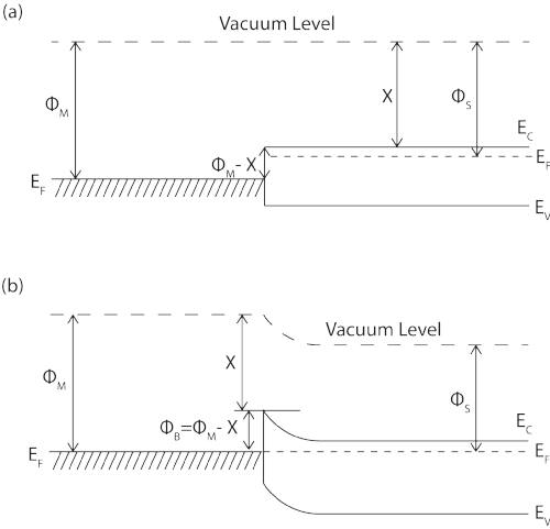 |
Figure 1: (a) An energy band diagram of an metal and an n-type semiconductor under non-equilibrium conditions. (b) an energy band diagram of a metal semiconductor contact in thermal equilibrium. |
The width of the Schottky barrier is dependent on, among other things, the doping density of the semiconductor. It is therefore possible, in the case of SSmS junctions, to tune the barrier in order to allow either more or fewer electrons to tunnel through.