
Resonant Tunnelling Diode
Introduction
The Resonant Tunnelling Diode (RTD) is a quantum well structure semiconductor device that uses electron tunnelling and has the unique property of negative differential resistance in its current-voltage characteristics. For certain applied voltages, increasing the voltage leads to a decrease in measured current. The IV characteristics of an RTD are shown in figure 1.

Figure 1: IV characteristics of an RTD, showing NDR
Operation and Band Structure
The band strucure of the RTD under different applied bias voltages is shown in figure 2 [1]. The device consists of two tunnel barriers enclosing a quantum well. Outside the barriers, doped contacts form a Fermi sea of electrons. Inside the well there is a resonant level of some small width. Under low bias voltage (Figure 2(a)), a small current flows due to non-resonant and scattering assisted tunnelling, leakage current through surface states and thermionic emission over the barriers. When the bias voltage is increased, the emitter level rises relative to the resonant level. Peak current (Figure 2(b)) is achieved when the emission region conduction band is at the same energy as the resonant level and the most electrons tunnel from the emission region into the resonant level. If the voltage is increased further, the resonant level falls below the emission region (Figure 2(c)) and the current is reduced, leading to the NDR property observed in figure 1. Eventually background effects dominate, and the current rises again as in a traditional resistor.
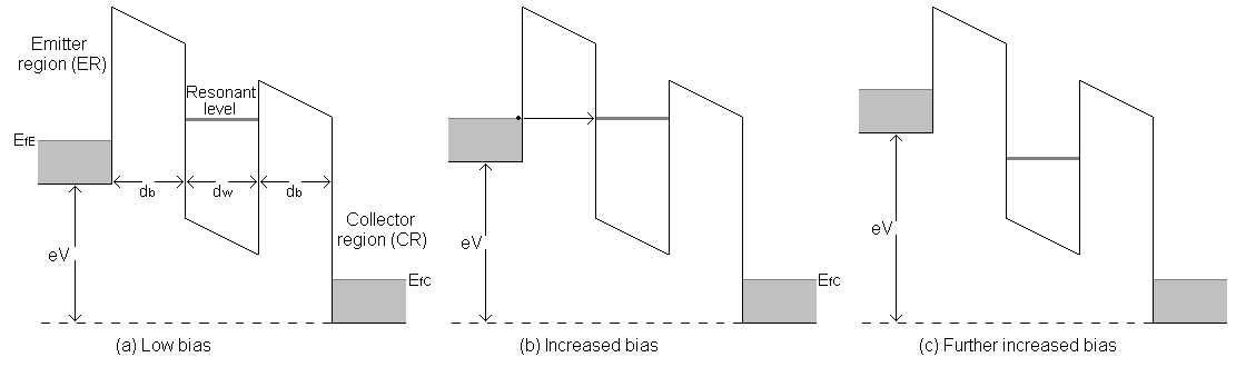
Figure 2: Band structure of the RTD under different applied bias voltages
NDR Research
The NDR device is of interest due its potential applications in high frequency oscillators, high speed switching and multi-level logic. The quality of fabricated devices can be described using the ratio of the peak and valley currents (PVR). Double barrier RTD devices have been grown by MBE from hexagonal AlN/GaN [2]. Research has shown that the performance of the device deteriorates as defect density increases and that the NDR effect is not reproducible. This is thought to be due to the charge trapping effect caused by the internal polarization of the wurtzite structure and defects. A higher quality device could be produced by MBE using cubic AlGaN/GaN. See the article on III-V Stuctures for a summary of the advantages of the cubic structure.
References
-
N. Zainal, Study of Cubic III-V Nitrides for Device Applications, University of Nottingham PhD Thesis (2010).
-
A. Kikuchi, R. Bannai, K. Kishino, Phys. Stat. Sol. (a), 188, 187, (2001).