
MBE
PVD - Physical Vapour Deposition
MBE - Molecular Beam Epitaxy
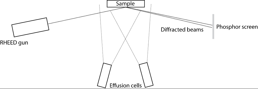
In MBE, material is sublimated (or evaporated in the case of a liquid source) from effusion cells, thus forming molecular beams that are incident upon a heated sample. A typical MBE vacuum chamber, with in-situ RHEED (reflection high-energy electron diffraction) included is shown in Figure 1.
 |
|
Figure 1: Simplified schematic of an MBE growth chamber with in-situ RHEED |
The sample consists of the substrate, onto which the material you wish to grow is deposited, with an included heater system and a system for rotating the substrate. Heater systems typically have one of two forms: resistive heating from a refractory metal filament or electron beam heating (these are described below). RHEED is described elsewhere.
Situated directly underneath the substrate are the effusion cells, which have shutters covering them to enable control over the atomic species being deposited. The effusion cells consist of a crucible containing the source material, typically constructed from pyrolytic boron nitride and a heating source. Heating is then typically performed by one of two methods, either ohmic heating from a filament wound around the crucible or by electron beam heating. In electron beam heating, thermionic electrons are accelerated toward the source material through a potential of a few kV and deposit tens of watts of power, inducing heating in the source material [1]. Typically the type of heating required is dictated by the flux of material required and the melting point of the materials. For example, indium has a low melting point (156 oC) but requires temperatures in excess of 700 oC to achieve a suitable flux, whilst tungsten, a refractory metal, requires temperatures over 2000 oC [2]. Consequently, resistive filament heating is suitable for the evaporation of indium but not for tungsten, where electron beam heating would be more appropriate.
As the molecules (in this discussion molecule will be used to mean either an atom or a molecule, as it is dependent upon the source material as to which is evaporated) reach the surface they have a probability of 'sticking'. Once a molecule has become attached to the surface there are several processes that can occur [3]. If it becomes adsorbed onto the surface through weak, physical, bonds such as van der Waals forces, then it is said to be physisorbed. If the molecule undergoes an electron exchange process and becomes chemically bonded to the surface, then it is said to be chemisorbed. If the molecule does not desorb then the energy available from the heated substrate will cause it to diffuse about on the surface, promoting growth. In order to form a crystallographically oriented material, incoming molecules must arrive or diffuse to epitaxial sites and become chemisorbed at that site.
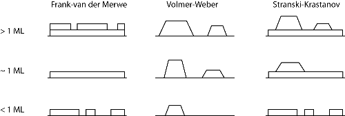
There are three main growth modes that can occur depending upon the substrate temperature, the deposition rate and available surface energy. These modes are illustrated in Figure 2.
 |
|
Figure 2: The three idealised growth modes: Frank-van der Merwe (layer-by-layer growth), Volmer-Weber (3D island growth) and Stranski-Krastanov (3D islands with a wetting layer). ML denotes a monolayer (approximately 1015 atoms). From [3]. |
Layer by layer, or Frank-van der Merwe, growth is the ideal mode for high quality thin films, since the next monolayer of material forms only after the first has finished. Volmer-Weber growth involves the formation of 3D islands on the surface. The final mode is Stranski-Krastanov growth and is an intermediate mode consisting of 3D islands with a wetting layer. Another, less common, form of growth termed endotaxy can also occur. This is where the overlayer grows into the surface due to large scale chemical intermixing and high reactivity [4].
Growth in MBE is entirely dependent upon the arrival of atoms at the surface and, as such, the quality of the growth material is highly sensitive to the arrival of impurity atoms. Unwanted background gases, such as nitrogen or oxygen, can have unwanted effects on the properties of the semiconductors and in order to overcome this problem the use of an ultrahigh vacuum system is necessary. Ultrahigh vacuum chambers, with background pressures in the range 108 to 1010 mbar, and low partial pressures of impurity gases such as water, CO and CO2. At atmospheric pressures the surface is contaminated by a single monolayer, approximately 1015 molecules cm2, of material in approximately 35 ns, however, at 10-9 mbar contamination occurs over a time period of approximately 3500 s [5]. This is considerably longer than the average growth time in MBE and so reduces the incorporation of impurities.
There are several variables within MBE, all of which can be independently adjusted and monitored in order to improve the quality of growth, these are:
- Flux rate (the number of atoms arriving at the substrate surface)
- Substrate temperature (affects diffusive properties of impinging atoms)
- Source temperature (speed of atomic arrival and flux rate)
The flux rate can be controlled by adjusting the evaporation/sublimation rate of the source materials, the source temperature whilst the substrate temperature is directly adjusted depending on the heating method used. The flux rate, and the source temperature, affect the growth rate as they influence the arrival rate of molecules at the surface. Typical MBE growth rates are 1 Å per second, this equates to one atomic layer per second. With the correct growth rates and having control of the molecular beams using the shutter systems, multi-layer structures can be grown reliably and repeatedly. Some substrates require particularly high temperatures during preparation and following growth. One such process is called annealing, in which the sample is again heated in order to recrystallise and repair damage to the crystal structure.
Depending on the type of growth there are advantages in favouring certain growth conditions. When growing III-Sb semiconductors, it is necessary to maintain low substrate temperatures as antimony is readily desorbed from the surface at larger temperatures. This is especially true for materials with low non-congruent temperatures. The non-congruent temperature is the temperature above which one atomic species is preferentially evaporated, often leaving non-stoichiometric material. The growth of strained layers requires lower substrate temperatures in order to reduce the diffusion of atoms on the surface. This reduces the probability of the layer relaxing and eliminating the benefits of introducing strain into the system. The disadvantage is that more defects are generated during growth due to the decreased mobility of deposited atoms, which typically need to move across the substrate in order to find the ideal 'epitaxial' site.
In general:
Higher temperatures result in more mobile surface atoms and thus more highly ordered material. The disadvantages are that interfaces become smoothed due to diffusion of atoms.
Lower temperatures generate more abrupt interfaces, which are often higher in quality, whilst the lower mobility of atoms introduces more point defects into the layer.
References
- A. Chambers, Modern Vacuum Physics, Chapman & Hall (CRC), 2005
- J. M. Lafferty, Foundations of Vacuum Science and Technology, Wiley-Interscience, 1998
- M. A. Herman and H. Sitter, Molecular Beam Epitaxy: Fundamentals and Current Status, Springer-Verlag, 1989
- W. Braun et al, J. Crys. Growth., 2007, 301-302, 50 - 53
- D. P. Woodruff and T. A. Delchar, Modern Techniques of Surface Science, Cambridge University Press, 2nd Ed., 1994
Bibliography
- A. Chambers, Modern Vacuum Physics, Chapman & Hall (CRC), 2005
- M. A. Herman and H. Sitter, Molecular Beam Epitaxy: Fundamentals and Current Status, Springer-Verlag, 1989
- K. Jousten, Handbook of vacuum technology, Wiley, 2006
- J. M. Lafferty, Foundations of Vacuum Science and Technology, Wiley-Interscience, 1998
- J. Y. Tsao, Materials Fundamentals of Molecular Beam Epitaxy, Academic Press, 1993
- D. P. Woodruff and T. A. Delchar, Modern Techniques of Surface Science, Cambridge University Press, 2nd Ed., 1994