
Growth of QDs
Growth
QDs can be fabricated by various techniques. They can be prepared for instance by lithography, molecular beam epitaxy (MBE), metalorganic chemical vapour deposition (MOCVD) and vapour liquid solid (VLS). Chemically they can be prepared through high temperature process e.g. QD incorporated in a glass matrix or other methods such as colloidal chemistry [1].
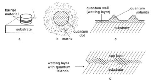
Fig.1 Various possibilities to form quantum dots by microstructuring of quantum wells (a), by precipitation in glasses or organic solutions (b) and by ¡¡ãselfassembly¡¡À (c, d) (schematic)
The first possibility is the micro- or nano-structuring of a quantum well by lithography and etching as shown schematically in (a). As for the wires, the lateral dimensions of the dots are usually considerably larger than the thickness of the well, leading to pancake-shaped dots, with the consequence that the quantization energy from lateral confinement is usually small compared to the one from the parent quantum well itself.
The other possibility is to grow QDs by an annealing procedure in glasses doped with the constituents of a semiconductor. This technique is widely used for II¡¡¡¡ì¬CVI compounds such as CdS1−xSex including the cases x = 0 and x = 1, for CdTe or for the Cu halides. The commercially available glass edge filters are made in this way. The average diameter of the dots increases with annealing time and temperature. We show schematically in (b) a high-resolution transmission electron (HRTEM) micrograph of a single dot in a silicate glass matrix. The lattice planes within the almost spherical nano crystallite are already visible.
Other techniques involve chemical precipitation of, for example, CdS in (organic) liquids or gels. These techniques have the advantage of giving dots that are almost spherical and have a high barrier, but the disadvantage is that one always gets a distribution of the dot radii with a certain width that is rarely below 10%. Since the quantization energy depends on the radius, this gives one contribution to the inhomogeneous broadening of the ideal ¦Ä-function density of states. Still another possibility is to grow the dots in the voids of zeolithe crystals or of synthetic opals
A topic that has recently gained interest is ¡¡ãself-assembled¡¡À quantum dots or thickness fluctuations occurring, e.g., for Ga1−yIny as wells under suitable conditions. In strongly lattice misfit systems (strong means a lattice misfit beyond about 5%), apart from the formation of misfit dislocations, the possibility of so-called Stranski-Krastanov growth mode, where small hillocks form on a wetting layer. In theses hillocks or small pyramids the growing layer relaxes towards its own lattice constant. These pyramids have been observed, e.g., by scanning microscopy (c). and a lot of effort has been invested in calculating the electron and hole eigenstates and energies in these structures including the spatially varying strain. The preferential systems in which these so-called self-organized quantum dots or better quantum islands (because of their rather flat island-like shape) are investigated are In1−yGayAs/GaAs including y = 0 and CdSe/ZnSe.
Then there come some drawbacks. It has been found by HRTEM investigations in both systems that during overgrowth a substantial intermixing between well and carrier material frequently occurs, with the consequence that the quantum islands consist in most cases of more pronounced thickness or composition fluctuations than well-defined pyramids after overgrowth, where they are no longer directly accessible to scanning microscopy (d).
References:
- Klimov, V. (2004). Semiconductor and Metal Nanocrystals: Synthesis and Electronic and Optical properties . New York: Marchel Dekker, Inc.