
What you need to control for bandgap engineering
Si is an abundantly available and hence cheap semiconductor material which has been used widely in industry. However, for certain optical applications, Si is not the most suitable material. It is for example not possible to make devices such as Single Photon Avalanche Detectors (SPADs) and Quantum Cascade Lasers (QCLs) operating at wavelengths between 1.3μm and 1.55μm with Si. Together with the desire to keep using existing fabrication facilities designed for Si devices for cost efficiency and the fact that Ge is a more expensive material, researchers have drawn their attention to Si1-xGex (0
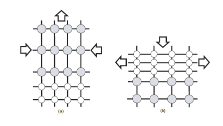
Figure 1. Schematic of layers under in-plane (a)compressive and (b)tensile strain. Layers with larger lattice constant are shown in grey. Adopted from [1]
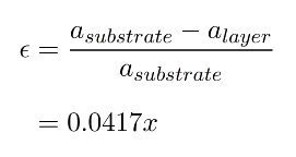
However, Ge has a lattice parameter of 5.658Å which is 4.17% larger than that of Si (5.431Å). So if one deposits a layer of Ge on top of Si, there will be a mismatch between both lattices and something should happen at or near the Si/Ge interface to make them fit together anyway. There are two things that can occur: the interface being under strain and the generation of so-called disclocations. A strain between two layers of material is simply a force acting in-plane which is compensated by the attractive/repulsive forces between the atoms in the lattice. If the two layers were separated, the atoms in each lattice would jump back to their lattice equilibrium positions. The strain, ε, in the layer due to the lattice mismatch (or misfit) can be expressed in terms of the lattice constants of the layer, alayer, and substrate, asubstrate:
For silicon-germanium strained layers, ε will vary with germanium composition from zero to 0.0417 and will be negative [positive] for compressive [tensile] strain. Suppose one deposits Ge on top of Si. Since the lattice constant in Si is smaller than that in Ge, the pre-existing Si layer will try to pull the atoms in the Ge lattice more closely togehter as to match its own lattice. See figure a). This is called compressive strain. If one deposits Si on top of Ge, the reverse will happen and this effect (figure b) ) is called tensile strain. Strain can be both an advantage and a disadvantage. As an advantage, one can exploit the fact that the band structure and Si and Ge change under strain, which makes it one method to do bandgap engineering: changing the bandgap by adjusting the strain. The so-called Vergard's law states that the lattice constant of an alloy XY is approximately the linear interpolation (weighted average with composition x) of the lattice constant of the separate materials X and Y. In the literature, a small quadratic correction to this law is incorporated.
When an external force is applied to give tensile or compressive strain to the crystal, the degeneracies in the conduction and valence band are broken. There are two components to the strain which changes the band structure of materials. Hydrostatic strain (due to the fractional volume change) shifts the energy of a band. Biaxial strain splits the degeneracy of bands e.g. the valleys in the conduction band of silicon/germanium and the degenerate LH and HH valence band edge.
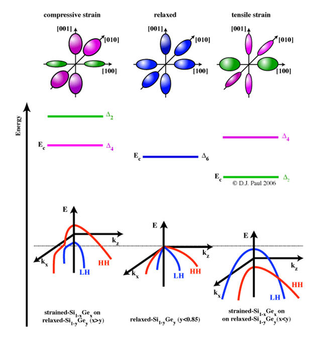
Fig 2.The hydrostatic shift and uniaxial splititing of the conduction and valence bands for (100) substrates for both compressive and tensile strain. Adapted from [2]
The conduction band of bulk Si/Ge is composed of a set of six-fold degenerate bands, Δ6, associated with electron transport along the six <001> crystal directions. The energy minima of each band forms an elliptical surface of constant energy in k-space, the surface area of which describes the number of momentum states available to electrons(see figure 2). Intervalley scattering occurs between all six ellipsoids as they are degenerate in energy. The application of strain in the x-y plane pseudomorphically deforms the crystaland breaks the degeneracy of the states into a four-fold and a two-fold set, denoted as Δ4 and Δ2, respectively. Under tensile strain Δ4 is reduced in energy, resulting in an energy gap between Δ4 and Δ2, which becomes larger with more strain. Occupancy of the lower energy bands is favoured, which reduces the total number of states electron can scatter into. Strain has a similar effect on the valence band in bulk Si/Ge, which is composed of a two degenerate bands for the transportation of light holes (LH) and heavy holes (HH), as shown in figure 2.4 (a). Tensile strain shifts the LH band to a lower energy (for holes energy is taken in the opposite sense to electrons) resulting in a strain dependant energy gap which reduces intervalley scattering as depicted in figure 2.4 (b). The spinorbit (SO) band is also shifted to a higher energy than the LH and HH bands, further reducing scattering. The reciprocal of the curvature of an energy band ( referring to the
curves in the figure above) is essentially the effective mass of the carriers occupying it. The curvature of the LH band (which shifts to a lower energy under tensile strain), is affected such that light holes become heavier than heavy holes. In the conduction band, a reduction in the curvature of the Δ2 bands also results in a reduction in effective mass. All the reduction in effective mass and increase in scattering time enhance mobility and are highly desirable for the manufacture of future electronic devices.