
Ultraviolet Photoelectron Spectroscopy
In X-ray photoelectron spectroscopy, high energy X-rays are used to probe the elemental distribution within a solid. In ultraviolet photoelectron spectroscopy (UPS), ultraviolet photons are used instead. The lower energy of the UV photons restricts their interactions to the valence band and, as such, provides an invaluable technique for probing the electronic structure of a solid.
UPS requires ultrahigh vacuum, so as to avoid the attentuation of emitted photons, an electron detector and a UV photon source. The photon source is often a helium discharge lamp, which has two energies, the HeI photon at 21.2 eV and the HeII photon at 40.4 eV. An alternative to using a helium discharge lamp is to use a monochromated synchrotron source, this offers large fluences and continuous, tunable, energies with little spread [1].
The typical path length of electrons released during UPS is of the order angstroms, making UPS highly surface sensitive. However, the path length is still sufficient for electrons originating inside the bulk of the solid to reach the surface and therefore be detected. Enabling the determination of the bulk-like band structure as well as surface specific electronic states. By considering the angular distribution of the emitted photoelectrons, it is also possible to map out the energy and momentum of electrons propagating inside the material [2]. This variation of the technique is known as angle-resolved UPS or ARPES.
In UPS, as in XPS, an incident photon ionises an atom resulting in the emission of a photoelectron. However, the lower energy of the photons used in UPS result in electrons coming from valence states in the solid. In XPS, the large (relatively to the binding energy of the valence states) energy results in very large electron kinetic energies and small photoionisation cross-sections for the valence levels. As a result the count rate of detected electron is low and the energy resolution is poor making it difficult to use XPS to investigate valence levels. The low energy of UPS photoelectrons is a strong advantage in the study of band structure and surface properties. However, this low energy is also disadvantageous due to the interference of final state effects. As the energy of the emitted electrons is comparable to those of the valence electrons there is a strong overlap of the initial and final wavefunctions of the emitted electron. The resulting counts versus energy spectrum is then a complex mixture of these states and in order to simulate such a system strong electron-electron correlations have to be accounted for.
An example UPS spectra is shown in Figure 1.
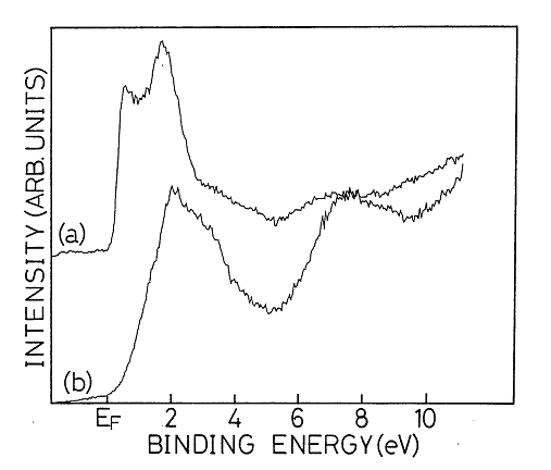 |
| Figure 1: Example UPS spectra for GaAs grown on Si, the two curves represent different growth patterns. From [3]. |
Notice that at a binding energy of 0 eV, which coincides with the definition of the Fermi energy, the intensity rapidly drops off to zero. As the valence states in a solid are the least energetic, they contain the most weakly bound electrons. These electrons are responsible for the vast majority of unique electronic and electrical properties in materials. As such, the valence bands contribute strongly to the density of states (DOS) around the Fermi level. Correspondingly, in UPS we probe the DOS at EF.
A DOS of zero at the Fermi level is a property of semiconductors and reflects the band gap. Equivalently, a metal has a finite DOS crossing the Fermi level giving rise to large values for conductivity and the large number of free charge carriers. By considering spin and other such effects a wide range of unique density of states can be found, giving rise to many different phenomena. One example of this is the half-metallic ferromagnets, the spin splitting at the Fermi level 100% polarised. For one spin orientation, called the spin majority direction, there is a metallic DOS at the Fermi level. Whilst for the other spin polarisation, the spin majority direction, there is a band gap and zero density of states. This mixture of metallic and semiconducting properties give rise to strong ferromagnetic behaviour and a 100% spin polarised material. This has widespread implications for the growing field of spintronics.
References
- D. P. Woodruff and T. Delchar (1994), Modern Techniques of Surface Science, Cambridge University Press
- A. Damascelli, Physica. Scripta., 109 (2004), 61-74
- K. Maehashi, S. Hasegawa and H. Nakashima, Jpn. J. Appl. Phys.(1993), 32, pp642-645
Bibliography
D. P. Woodruff and T. Delchar (1994), Modern Techniques of Surface Science, Cambridge University Press