Silicon Photonics
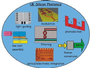
Warwick was part of the £5M EPSRC funded initiative UK Silicon Photonics led by Prof Graham Reed at Surrey University (now Southampton) and also included the universities of Leeds, St. Andrews and Southampton together with QinetiQ and IMEC.
 Silicon Photonics promises to revolutionise the next generation of ICs by providing solutions for optical interconnections between chips and circuit boards, optical signal processing, optical sensing, and the so called “lab-on-a-chip” biological applications. It is also expected to provide low cost optical signal processing chips that will interface with optical fibres brought directly to the home that can take advantages of the enormous bandwidth of Fibre-To-The-Premise (FTTP) technology. Services such as video-on-demand, high speed internet, high definition TV and IPTV, that require large bandwidths, may also expand dramatically as a result of this work. Silicon is the material of choice for the microelectronics industry, partly due to the cost effective way in which it can be processed. Therefore, integrating both optical functionality and electrical intelligence into the same silicon chip is expected to deliver a cost advantage as compared to more conventional optical technologies.
As part of the UK consortium, this project developed material structures and associated epitaxial process routes required for an integrated Ge optical detector. Initial work will be on isolated detectors for light collection from a free space transmission path, leading ultimately to a fully integrated detector coupled by Si waveguides to a silicon based light source on the same chip. Unstrained Ge layers will be grown by CVD directly on (100) Si wafers using a Ge seed layer to induce relaxation on the Si substrate yielding smooth layers. Strained (and unstrained) Ge layers will also be produced by growth on Warwick’s ultra-low defect SiGe virtual substrates. By producing the right layer structure, with very smooth interfaces, it is possible to confine and/or control both electrons and photons. As a second part of this project we will use the quantum confined Stark effect to build optical modulators based on Si/Ge superlattices - leading to another key element of the silicon photonic system.
Project details
| Sponsor | EPSRC EP/E065317/1 |
| Title | UK Silicon Photonics |
| Dates | July 2008 to June 2013 |
Links to collaborators
- University of Surrey , Advanced Technology Group
- University of St Andrews, Microphotonics and Photonic Crystals Group
- University of Leeds , Institute of Microwaves and Photonics
- Southampton University
- QuinetiQ
Watch iCast relating to Si Photonics 
![]()

